


Telluride 碲化物
- 公司名称 上海巨纳科技有限公司
- 品牌 其他品牌
- 型号
- 产地 美国
- 厂商性质 生产厂家
- 更新时间 2018/7/11 9:27:10
- 访问次数 778
联系方式:袁文军13761090949 查看联系方式
联系我们时请说明是化工仪器网上看到的信息,谢谢!
| 供货周期 | 一周 |
|---|
Our R&D team are about to release new Tellurene nanowires series (in late March,2018), you may pre-order these products when order regular Tellurene single crystals.
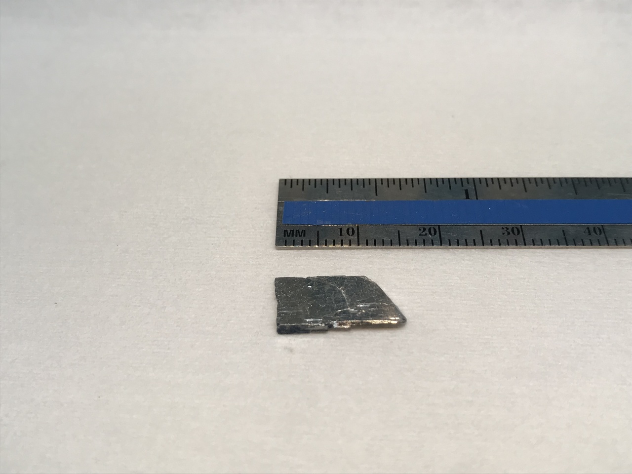
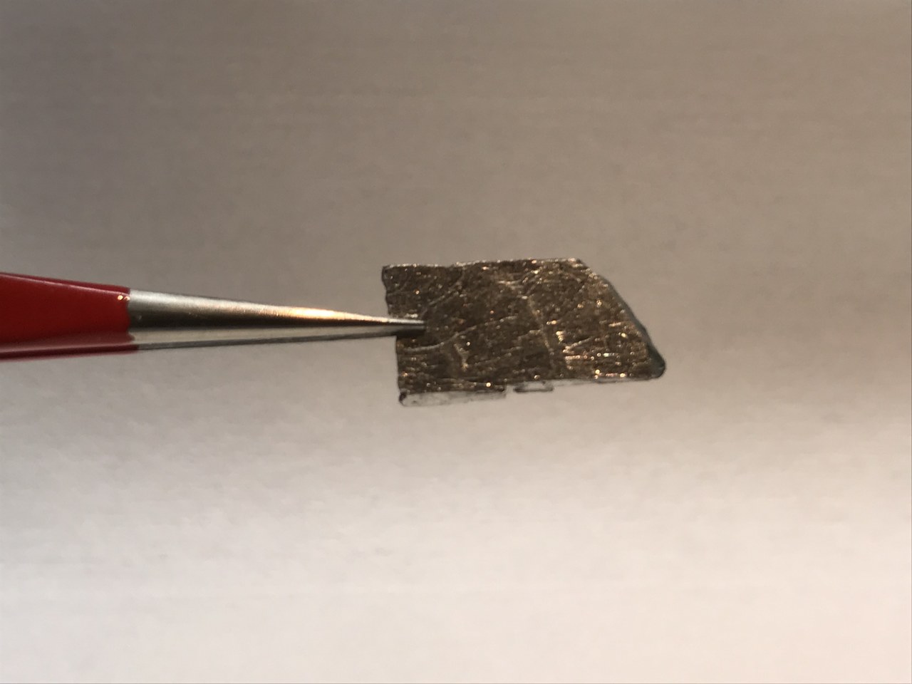
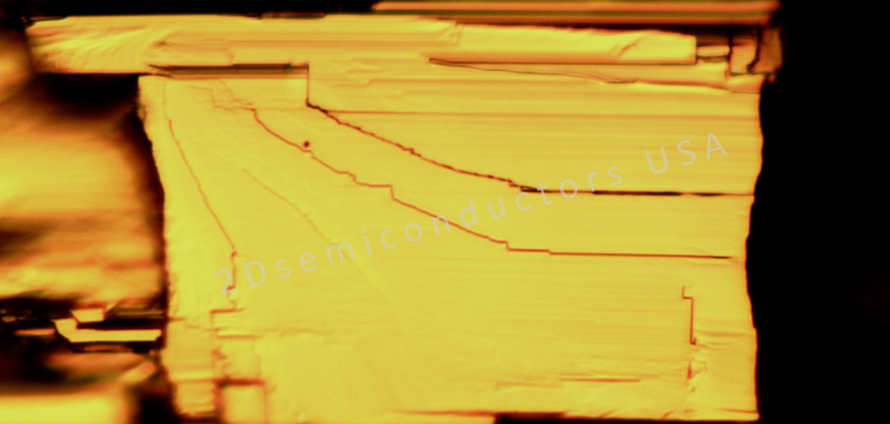
The first commercial vdW Tellurium (b-phase) crystals. Layered tellurium crystals have been synthesized in perfectly vdW order through flux zone growth technique. The crystal has 99.9999% (6N) rated purity and has been crystalized in perfect atomic order.
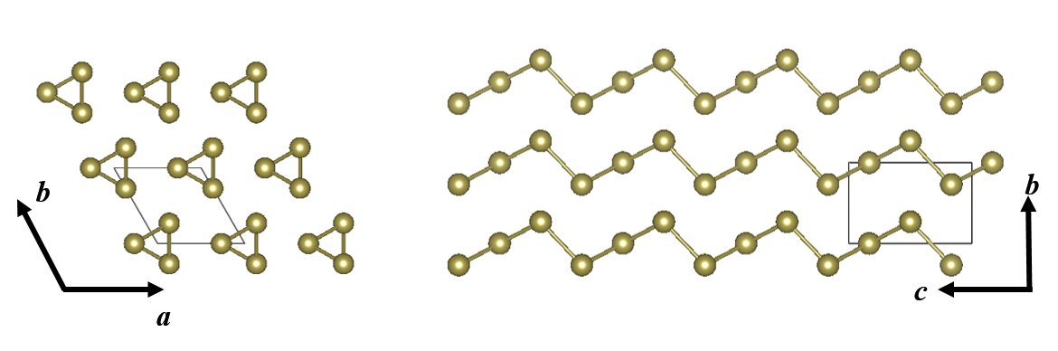
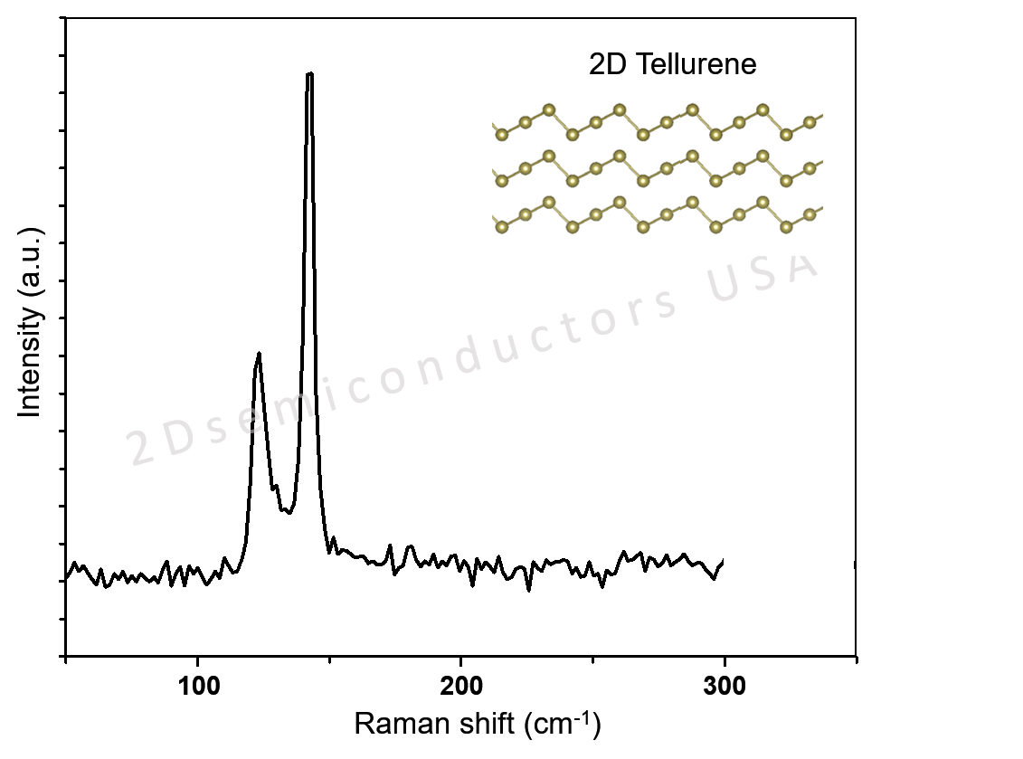
Layered tellurium (Te) has a trigonal crystal lattice (see product images) in which individual helical chains of Te atoms are stacked together by van der Waals type bonds and spiral around axes parallel to the [0001] direction at the center and corners of the hexagonal elementary cell [1-2]. Tellurene exhibits a tunable bandgap varying from nearly direct 0.31 eV (bulk) to indirect 1.17 eV (2L) and direct at 1.3 eV (1L) [3]. It has four (two) complex, highly anisotropic and layer-dependent hole (electron) pockets in the first Brillouin zone with an extraordinarily high hole mobility reaching up to theoretical ∼1E5 cm2/Vs value [1-3].
Material characteristics
High carrier mobility semiconductor
Tunable IR semiconductor (Eg ranging from 0.3 to 1.3 eV from bulk to monolayers)
2D anisotropic semiconductor
Physical size ~1cm or larger;
Note: This product is same as tellurene material. While material itself is perfectly crystallized in trigonal form (weakly coupled Te chains are present), it is inherently harder to exfoliate in comparison to graphene or MoS2. For best results, we recommend using strongly adhesive tapes or liquid exfoliation technique.
Related references
[1] "Two-dimensional tellurium" Nature 552, 40-41 (2017)
[2] "Large-area solution-grown 2D tellurene for air-stable, high-performance field-effect transistors"; arXiv:1704.06202
[3] "Few-layer Tellurium: one-dimensional-like layered elementary semiconductor with striking physical properties" ; https://doi.org/10.1016/j.scib.2018.01.010

 采购中心
采购中心
 化工仪器网
化工仪器网